Electronics Notes...
Page Contents
References
- Capacitor i-v equation in action, Khan Academy.
- Derivation of Charging and Discharging Equations for RC Circuit, JKTekker, YouTube.com.
- Deriving the formula from scratch' for charging a capacitor', StackOverflow.
- What exactly is a current source?, StockOverflow.
- Battery Internal Resistance, LeanAboutElectronics.com.
- Essential & Practical Circuit Analysis: Part 1- DC Circuits, Solid State Workshop, YouTube.com.
- NPN Curves (seems broken?)
- Electricity & electronics - Robotics, learn by building, Ian Juby, Udemy.com.
- Introduction to NPN Transistor, The Engineering Projects.
- Transistor Configurations: circuit configurations, ElectonicsNotes.
- 2N2222; 2N2222A Data Sheet, Philips Semiconductors.
- NPN Transistor, ElectronicsTutorials.
- Circuit Lab Website.
- Ultimate Electronics eBook.
- Calculating resistor value for transistor, StackOverflow.
- Common Emitter Connection (or CE Configuration), Circuit Globe.
- Sign convention for passive components, Khan Academy.
- Labeling Voltages, Currents, and Nodes, Ultimate Electronics eBook.
- The Great "Power Vs. Energy" Confusion, Rob Lewis, CleanTechnica.
- Electric potential energy, Khan Academy, YouTube.com.
- Textbooks way of determining KVL polarities', StackOverflow.
- Electricity And Magnetism, HyperPhysics
Charge, Current, Voltage, Power
References
- The Great "Power Vs. Energy" Confusion, Rob Lewis, CleanTechnica.
- Electric potential energy, Khan Academy, YouTube.com.
- Essential & Practical Circuit Analysis: Part 1- DC Circuits, Solid State Workshop, YouTube.
- Electricity And Magnetism, HyperPhysics
Conventional Current And Charge
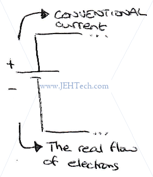 Historically positive charge moves through the circuit from the positive to negative terminals. This is called conventional current.
We now know that it is, in fact, the flow of electrons from the negative to positive terminals that is current. Due to the historical precedent,
current is still often shown as conventional current.
Historically positive charge moves through the circuit from the positive to negative terminals. This is called conventional current.
We now know that it is, in fact, the flow of electrons from the negative to positive terminals that is current. Due to the historical precedent,
current is still often shown as conventional current.
From Wikipedia: Conventional current flows from the positive pole (terminal) to the negative pole. Electrons flow from negative to positive. In a direct current (DC) circuit, current flows in one direction only, and one pole is always negative and the other pole is always positive. In an alternating current (AC) circuit the two poles alternate between negative and positive and the direction of the current (electron flow) reverses periodically.
.
Informally, current is a flow of electric charge.
Current,
We can integrate the above to get
Electric Fields, Energy, Work & Voltage
Let's revisit the terms energy, work and power.
Energy is the ability to do work.
Work is the force that must be exerted to move a mass a certain distance.
Power is the rate at which energy is generator/consumed.
Energy & Work
Energy is defined as the ability to do work. Work is what transfers energy from one form to another (energy is never destroyed). For example, work can turn potential energy into kinetic energy.
Energy is measured in Joules. 1 Joule is the energy transferred when a force of 1 Newton is applied to an object and moves it through a distance on 1 meter.
Work is defined as...
Power
Power gives that rate at which energy is used/produced. Power measures how fast the work gets done. Put another way, working faster == more power.

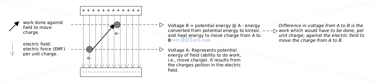
Electric Fields
Electric fields are created by charges. The field itself produces an electric force per unit charge, the direction
of which is defined as being the force it would exert on a positive test charge [LINK].
But what is force? It is measured in Newtons, where 1 Newton is the force required to give a 1 kg mass an acceleration
of 1 meter per second per second. I.e.
Voltage
Voltage,
If we integrate both sides of the abote w.r.t to charge we get:
Note that voltages are relative, which is why the negative terminal of the battery can be negative - it depends what the reference voltage you are measuring against is - e.g. if ground is midway between the two terminals then they will have voltages -A and +A respectively.
Energy & Power In Terms Of Current & Voltage
Give these definitions we can see how they are defined for electronics. Using some crude (read incorrect as we're using multiplication not integration to make it seem simpler) we see:
When current flows through a resistor it dissipates power in the form of heat. When it flows through an LED it dissipates power in the form of both heat and light.
Power, measured in watts, is also defined as:
Resistors usually have a power rating (the power they can dissipate) associated with them. This means that if you know the resistor's power rating you can calculate the maximum voltage or current you can put across/through them without breaking the resistor.
Note that electric potential energy is measured with respect to a reference point. In the image below one can see that the voltage either side of the resistor is measured w.r.t ground. Ground is the normal reference point, but any point in a circuit can be used as long as it is used consistently.

Note then, that potential difference, is the difference between to points, each of which has a potential energy w.r.t to a reference. The potential difference is the difference between these two points, but only make sense if the potential of each point is measured w.r.t to the same reference.
Ohm's Law
Ohm's law gives the relationship between voltage, current and resistance:
Passive Sign Convention
See the following references:
- Sign convention for passive components, Khan Academy.
- Labeling Voltages, Currents, and Nodes, Ultimate Electronics eBook.
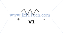
"Passive" describes components that do not create power and do not amplify signals. For example, resistors, capacitors and inductors are passive components because they do not create power and do not amplify signals.
Sometimes a voltage source, like a battery, can be said to be passive because although it creates power it does not amplify signals.
The sign convention for passive components is that the current goes into the positive terminal (terminal with higher V).
When analysing a circuit, as we'll see below when using Kirchhoff's laws, we have to label each component with a voltage and current. The passive sign convention makes sure that when we use Ohm's law, it comes out with the correct sign.
Take the following resistor. If we label the voltage across it as so:
We then know that, using the passive sign convention, that the current must be labelled so that it flows into the positive terminal, like so:
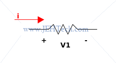
We're clearly talking about conventional current here, by the way.
What it means is that if we labelled either the voltage or the current incorrectly, Ohm's law will give a negative answer, because if we label the current going into the negative terminal, we must consider it to be negative current as it is going in the wrong direction. Why would we label a circuit wrong? Because sometimes in circuit analysis we do not know the polarity of an element, so we just guess, and then if the sign comes out negative we know we labeled the polarity wrong and change the labelling.
The convention to label current as positive when flowing into the + terminal is arbitrary, but it makes a few things work out simply and consistently:
- First, V-I relationships like the definition of Ohm's Law don't need a minus sign.
- Second, power consumption is defined correctly with
, where for ordinary components which are consuming power like a resistor, and for components which are supplying power like a battery.
Why would incorrectly labelling a branch (i.e., we labelled the terminal that current was going into as negative (-)) require a sign change? Simply because of this convention! If current moving in one direction is positive then moving in the other direction must be negative!
Kirchhoff's Laws
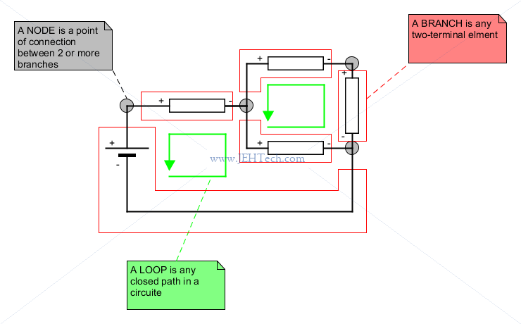
Nodes, Branches and Loops
Branch: A branch represents a single element such as a resistor. I.e., any two terminal element.
Node: A node is the point of connection between 2 or more branches. Every point going into the node, at the node, is at the same potential.
Loop: A loops is any closed path in a circuit. Starts and ends at the same node and does not pass through a node more than once.
The Laws...
Two important laws: Kirchoff's voltage law and Kirchoff's current law.
KCL
Kirchoff's current law says that the sum of currents flowing into a node must equal the sum of currents leaving a node. This is often expressed in another way: the sum of currents entering and leaving a node must always be zero. This works because we label, by convention, all currents entering the node as positive and all currents leaving the node as negative.
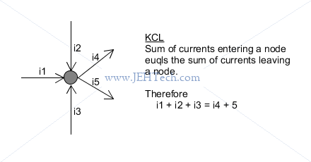
This can be written most compactly as:
Lets look at the following example [Ref]:
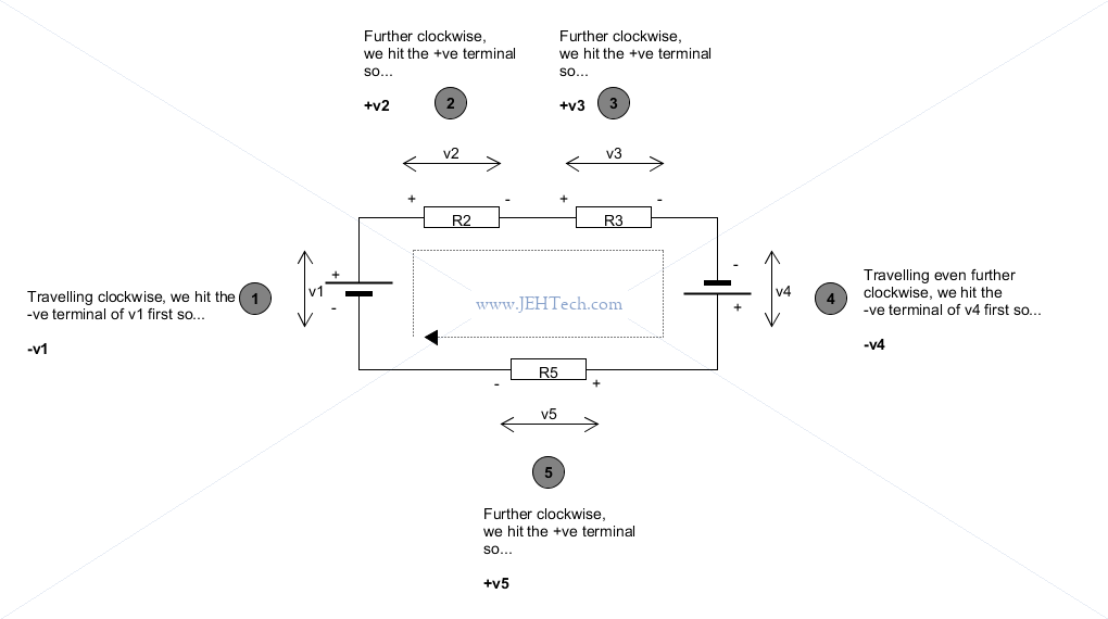
KVL
Kirchoff's voltage law says that the sum of voltages around a closed circuit must be zero, where the sign on each voltage is the polarity of the terminal encountered first as the loops is traveled around. Another way of saying it is that one way to assign the +'s and -'s is [Ref]:
- if the positive (+) side of the voltage is encountered first, assign a positive "+" sign to the voltage across the element.
- If the negative (-) side of the voltage is encountered first, assign a negative "-" sign to the voltage across the element.
However, for passive components, one might not know apriori how to label the terminals. The choice can be arbitrary, so long as the passive sign convention is used, such that in a loop, because we know current can only flow in one direction, whatever arbitrary direction we decided to think of it as going, if it enters the positive terminal then the result is a positive current, otherwise it is a negative current. We will see an example below.
This can be written most compactly as:
Say, for example, that
In this example it was trivial to know, apriori, what direction the current would flow. Sometimes we may not.
Example #1
The following is a simple example from the book "Fundamentals of Electric Circuits", fourth edition. This demonstrates the way that passive components can have their terminals labelled in an "arbitrary" fashion of our choosing (as long as we consistently apply the passive sign convention to know whether current is + or - whilst considering each branch). It stumped me for a while, so I asked, and got some very helpful answers on good old StackOverflow.
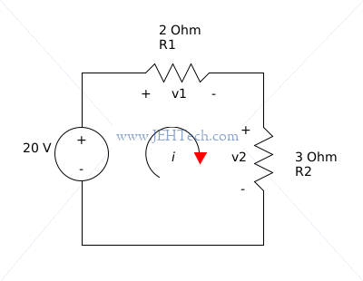
Conventional current flow is used, as indicated by the circular arrow. Going around the loop, because the current enters the negative terminal of R2, the current current and voltage must be negative!. See the section "Passive Sign Convention" above.
By Ohms, law
So, going around the loop we get
We know that the voltage drop across
Example #2
Another example. In this example we are required to find the voltage supplied by the voltage controlled voltage supply,
which provides
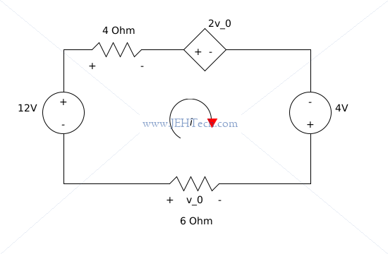
The power supplies can use the polarities already indicated on them. The resistors we can assign polarities arbitrarily to, but the ones shown are the ones shown in the book's example, so lets use them!
Using KVL:
Voltage v.s. EMF
The difference between voltage and EMF is that EMF is the ideal potential difference provided by a power source, whereas voltage is the effective potential difference provided by a source taking into account parasitics like equivalent series resistance (ESR) and so on.
EMF is the energy supplied per unit charge by a source (like a battery or generator), it is the cause of current.
Voltage is the electric potential difference between two points in a circuit, it is what you measure across components.
In a real battery, the terminal voltage is usually less than the emf when delivering current because of internal resistance.
Reference: OpenStax University Physics Volume 2, section on EMF and terminal voltage.
Resistance
Resistors control the current that flows through a part of a circuit, as described by Ohm's Law (
Resistor Colour Codes
In the drawing to the left you can click on the value-boxes to change the colour bands on the resistor to find out the resistance represented by the colour encoding. Note it only shows a 4-band resistor. 5 and 6 colour bands are possible but not shown here.
Note: Sometimes the click event on the canvas doesn't fire... not quite sure why that is. If first click doesn't work, persevere :)
Some popular ways of remembering the resistor colour codes include "Bad Boys Ravish Our Young Girls But Violet Gives Willingly" and my fav, "Bad Booze Rots Our Young Guts, But Vodka Goes Well".
Resistor's In Series
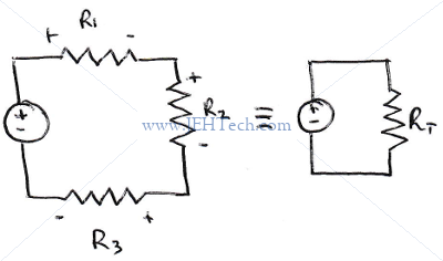
Resistors in series can be "collapsed" into an equivalent single resistor with a resistance that is the sum of all the resistances of the individual resistors.
Using Kirchoff's voltage law:
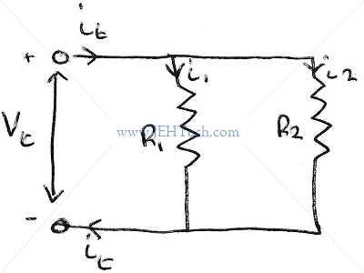
Resistor's In Parallel
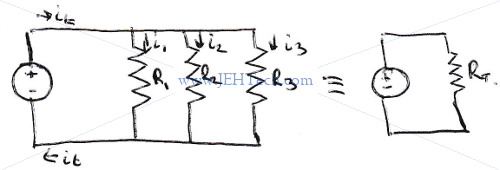
Resistors in parallel can also be "collapsed" into an equivalent single resistor...
Using Kirchoff's current law we can say that
Voltage Divider
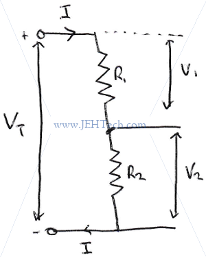
Using Ohm's law we know the following.
One issue to be aware of is that any load placed across
Current Divider
The Wheatstone Bridge
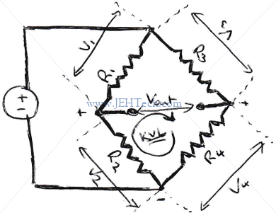
The Wheatstone Bridge is a circuit for measuring resistance very accurately. This material is based on the link to the Texas Instrument tutorial...
Using Kirchoff's voltage law around the loop consisting of
Let's say that we don't know the resistance of
A simple re-arrangement gives us...
In the above,
And now we can calculate the unknown resistance... why is this useful? Because this unknown resistance is our sensor. It could be a thermistor, LDR, or whatever... something that changes resistance due to the thing we're trying to measure.
One thing to note is that the
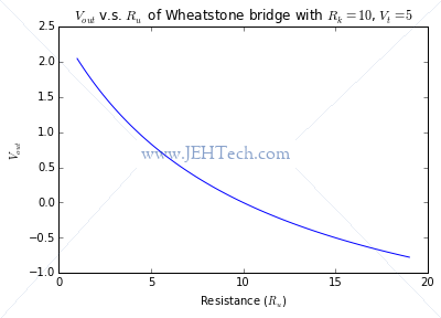
So... why use this rather complex arrangement to measure an unknown resistance when we could do the same using a simple voltage divider? The answer lies in the sensitivity of the measurement system. This is covered in the next section.
Voltage Sources & Current Sources, Ideal v.s. Real World
Voltage Sources
An ideal voltage source is one that supplies constant potential, no matter what load is connected to it. I.e., it produces whatever current is necessary to maintain the voltage across it [Ref]:

But, batteries, even power supplies etc etc are not ideal. In the real world they have a small internal resistance, anywhere between approx 0.1 Ω to 2.0 Ω depending on the battery [Ref], which means they are modelled more like this:

It can be seen that because the internal resistance of the battery, is in series with the circuit it is powering, i.e., the load (simulated by the resistor), the combination acts like a voltage divider, and so the voltage across the load varies with its resistance. I.e.,the battery is not ideal (but its pretty close!)
This is why it is always best to measure the voltage across a power supply when it is under load.
We can now also understand that an ideal voltage source is one that has zero internal resistance.
Current Sources
An ideal current source is one that always produces the same current, no matter how the voltage across it or the resistance of the load it is "feeding" varies, [Ref].
This is why, incidently, in a circuit you cannot have two current sources in series!
Source Transformations
It is possible to switch out a voltage source in a circuit for a current source and vice-versa using source transformation using Thevenin and Norton equivalent ciruits [Ref].
Superposition
Circuits can have multiple sources. In this case, to determine voltage levels at nodes, the principle of superposition can be used:
- Set all sources to zero except one,
- Solve the necessary currents and voltages using only that source,
- Repeat the above step for each source
- Add the circuit values together - "superimpose" them onto one another.
Take the following example [Ref]:

In the above diagram we get:
References
- What Exactly Is A Current Source?, StackOverflow.com.
- Battery Internal Resistance, LearningAboutElectronics.com.
- Essential & Practical Circuit Analysis: Part 1- DC Circuits, Solid State Workshop, YouTube.
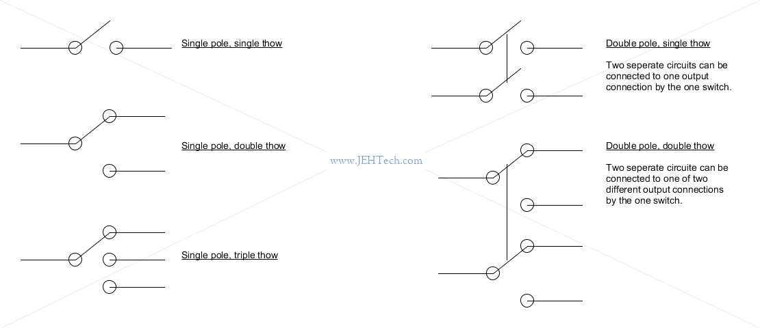
Switches
Switches are defined by the number of poles and throws they have...
Poles: A switch pole refers to the number of separate circuits that the switch controls.
Throw: The number of throws indicates how many different output connections each switch pole can connect its input to. Think of it as how many places a single source can be "thown to".
Capacitance
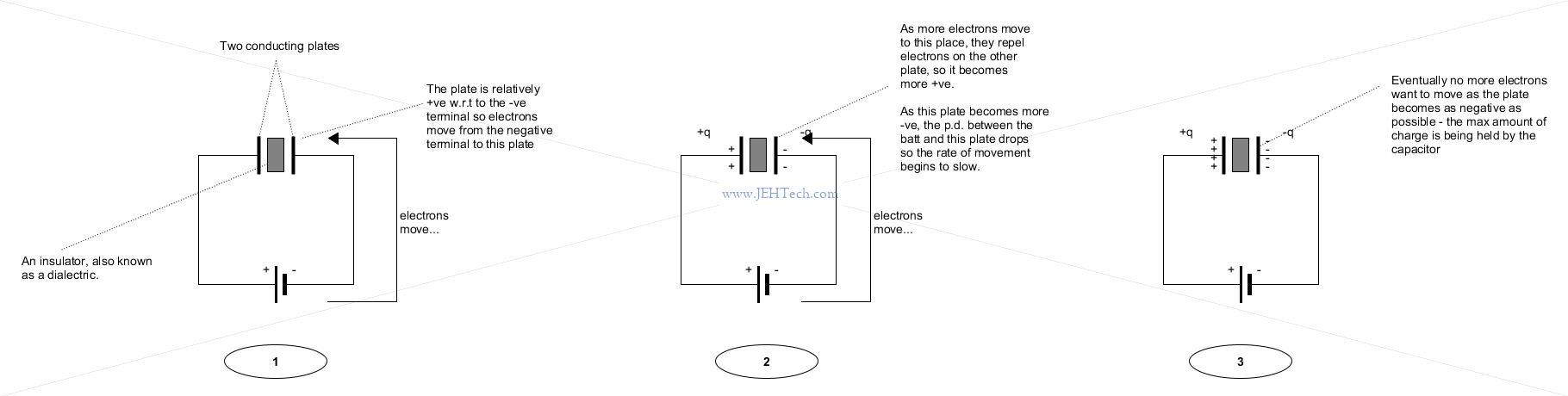
A capacitor consists of two conducting plates separated by an insulator (a.k.a. a dielectric).
When connected to a voltage source, the source creates a positive charge on one plate and a negative one on the other plate:
Charge stored is proportional to applied voltage:
Although, for equations etc., Farads are the expected units, in electronics capacitors in the range of nano-Farads to milli-Farads are used. Even milli-Farads are less common. More common are nano and micro-Farads.
By re-arranging the above we can see that capacitance is the charge per volt that the capacitor can store. Thus, the more charge that the capacitor stores per volt, the higher its capacitance is. This quantity is dependent on the type of dielectric used, the surface area of each plate and the distance between the plates.
Recall that current is the amount of charge that moves past a point per unit time. Thus,
by differentiating w.r.t time, the above, we get the current-voltage relationship of a cap:
Note that real capacitors dissipate their energy over time - they "leak"
Capacitors resist abrupt changes in voltage, which is why the function as low pass filters.
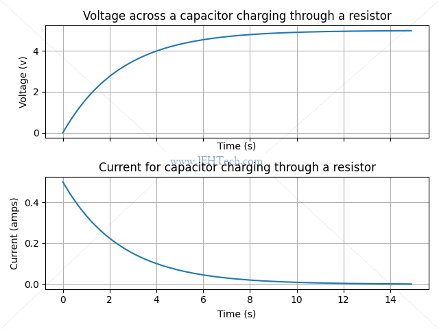
Example graphs showing voltage across a capacitor whilst charging and current over time:
Energy And Work
We had previously defined work as
Thus, the work required to charge a capacitor, i.e., the work done by the power source, is:
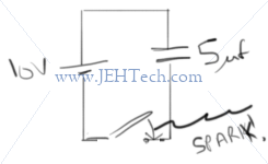
Charging Without A Resistor Means Trouble
If a capacitor is charged without a resistor to limit current the circuit will, at the beginning of the charge, be a short circuit. In the diagrams above, a spark will be seen at the switch which will dissipate some of the energy. As we will see below, exactly half of the energy is dissipated in the spark and that the maths kinda fails for this scenario...
Take the following example...
We know the work done by the capacitor when it discharges is defined as follows, giving the following result.
Charging Through A Resistor
When a capacitor, with a capacitance
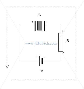
Recall KVL: the sum of voltages around a closed circuit must be zero. The dotted arrow
in the diagram above shows a direction around a closed ciruit, which by KVL means that [Ref]:
Now a quick aside to derive something we're going to need:
Recall:
Now we can continue by substituting
We end up with:
When selecting the resistance through which to charge a capacitor consider:
- Charging time - how quickly do you need it to charge?
- Capacictor specs - maximum rated currents etc.
- Power source limitations - maximum current supply can provide.
- Steady state current - don't want too large a voltage drop over in-series resistor so that charging is efficient but not so small that current is excessive.
In-series resistor could be anywhere between a hundred ohms to a couple of kilohms...
Reactance
The reactance of a capacitor,
So the reactance, or opposition to change in current, decreases with as frequency and/or capacitance increases.
This means that the smaller the capacitor the higher the reactance for a given frequency.
For a given capacitorance, the reactance decreases as frequency increases.
Current Leads Voltage
For capacitors thing "ICE": current (I) leads voltage, or E.M.F (E):
Capacitors In Series
Capacitors In Parallel
Reactance
See Current Lead And Lag, David Darling.
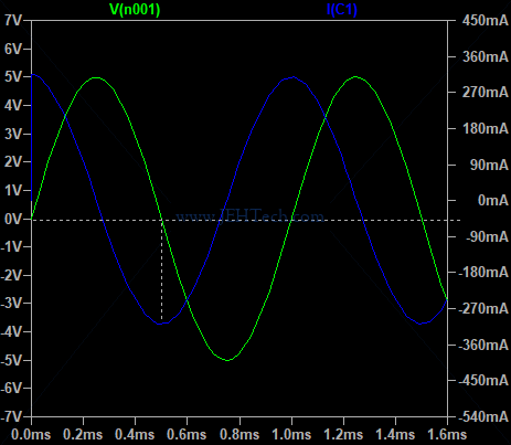
The opposition to the flow of alternating current due to capacitance is called "capacitive reactance.". In capacitors, the current leads voltage by 90 degrees. Resistance is measure using real numbers but reactance is measured in the complex plane.
When a capacitor is uncharged, the voltage across it is zero. The increasing voltage from the AC supply will therefore, at the start, deliver the maximum amount of current. As the voltage across the capacitor grows in opposition to the supply, the current flow will decrease. Therefore at the start there must be minimum voltage across the capacitor, bu maximum current flow from the battery. Because the AC voltage is sinusoidal, this means that the current and voltage must be 90 degrees out of phase and the current leads the voltage.
We know
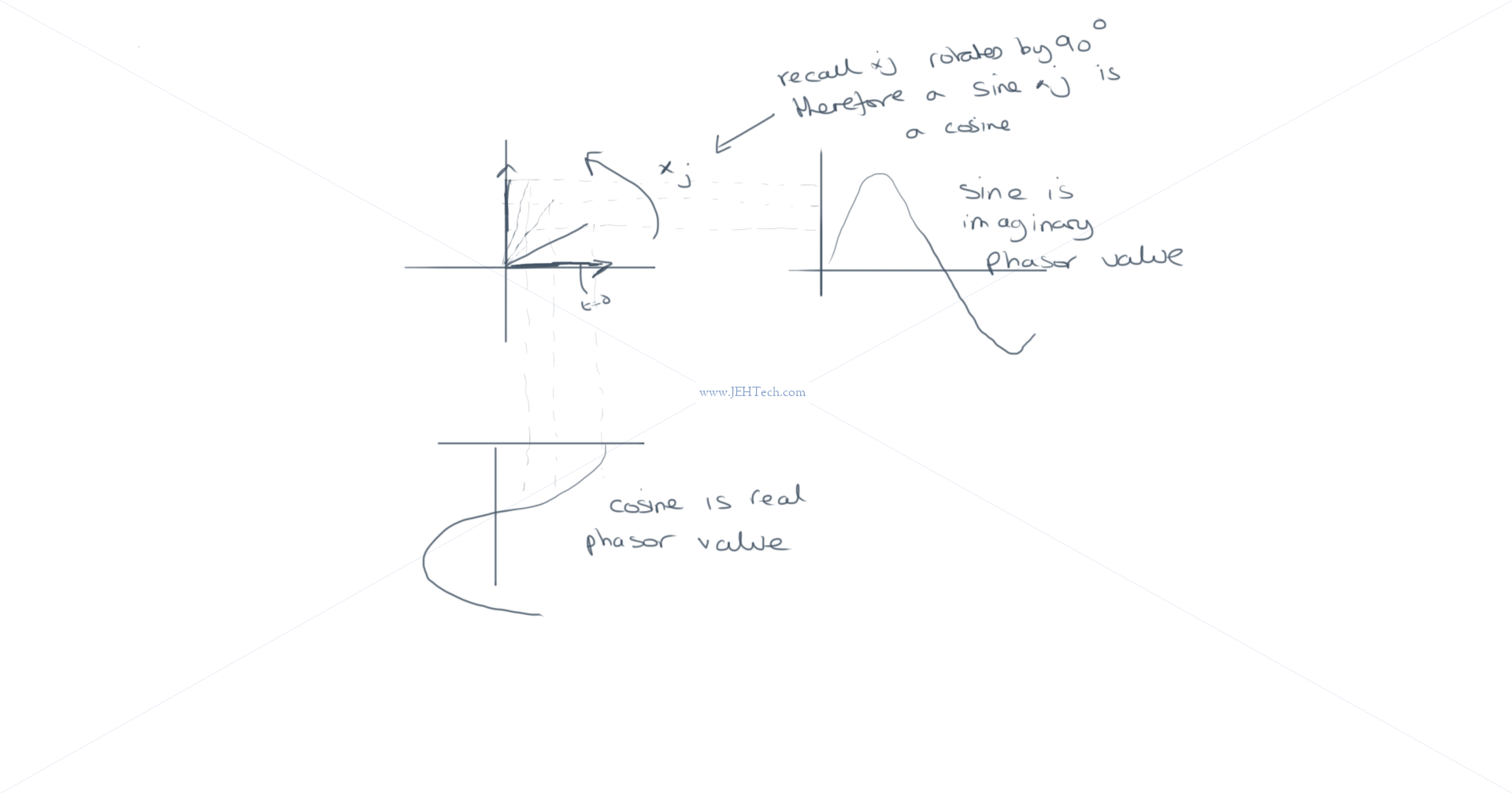
So, to eliminate the sinusoids, we could express sine as a rotation of a cosine. TODO
Parasitics
"Parasitics" are things that happen in a circuit that you didn't design on purpose, but are there anyway because real parts aren't perfect. Capacitors are not perfect. Their parasitics are represented like this (there are probably more complex models):
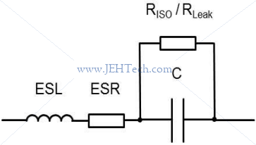
ESL stands for equivalent series inducance. Its a small inductance that every real capacitor has because of its leads, internal wiring, and layout. It acts like a tiny inductor in series with the component and can cause voltage spikes or ringing at high frequencies, especially in switching circuits.
ESR for equivalent series resistance. It represents losses inside the component due to the material and construction. High ESR can cause heat generation and affect stability in voltage regulators.
RISO and RLeak refer to the insulation and leakage resistance. Insulation resistance is the resistance of a dielectric (insulator) between conductors. Leakage resistance is the actual resistance that allows tiny unwanted current to flow through a capacitor or insulating material.
So, the lower the ESL, ESR and higher the RISO and RLeak, the better the capacitor.
Materials
Some common kinds...
| Capacitor Type | Advantages | Disadvantages | Common Uses |
|---|---|---|---|
| Film | Stable capacitance, low ESR, long life, high voltage rating, low dielectric absorption, non-polarized, good pulse handling, low noise | Larger size for high capacitance, more expensive than electrolytics for same capacitance | AC filtering, precision timing circuits, audio circuits, pulse circuits, snubber circuits |
| MLCC (Ceramic) | Small size, low cost, high capacitance per volume (low voltage), non-polarized, high reliability | Capacitance varies with DC bias and temperature, microphonic effect, limited high-voltage options | Decoupling, bypassing, RF circuits, high-frequency applications |
| Aluminum Electrolytic | High capacitance, cheap, good for bulk energy storage, high energy storage | Polarized, short lifespan, poor stability, high ESR, limited high-frequency performance | Power supply filtering, bulk energy storage, smoothing DC voltage |
| Aluminum Polymer | Low ESR, longer life, stable capacitance, high ripple current, high temperature tolerance | Lower capacitance per volume than standard electrolytic, higher cost, voltage limits | Switching power supplies, DC-DC converters, high-frequency circuits, automotive electronics |
| Aluminum Hybrid Polymer | Low ESR, high capacitance, longer life than standard electrolytic, good ripple current handling, moderate temperature stability | Higher cost than standard electrolytic, less stable than film or MLCC, voltage limits | Power supply filtering, high-capacitance applications needing better lifetime and ripple performance, automotive electronics |
Decoupling Capacitors
A lot of the capacitors you see in circuits, especially those featuring an integrated circuit, are decoupling. A decoupling capacitor's job is to supress high-frequency noise in power supply signals. They take tiny voltage ripples, which could otherwise be harmful to delicate ICs, out of the voltage supply.
In a way, decoupling capacitors act as a very small, local power supply for ICs ... If the power supply very temporarily drops its voltage (which is actually pretty common, especially when the circuit it's powering is constantly switching its load requirements), a decoupling capacitor can briefly supply power at the correct voltage. ...
The performance of many circuits is impaired by the presence of HF noise on their supplies, so any HF noise which might be present on an IC's supply must be shorted to ground. We cannot use a conductor for this as it will short circuit dc and blow fuses, but a capacitor (usually in the 1-nF to 100-nF range) blocks dc while acting as a short circuit for HF.
1 cm of wire or PC track has ~8 nH inductance (5 Ohms at 100 MHz), which is scarcely a short circuit. A capacitor acting as an HF short circuit must have low lead and PC track inductance, so each supply capacitor must be located very close to the two terminals of the IC it is decoupling. It is also important to choose capacitors with low internal inductance - usually ceramic ones.
And then this rather more friendly version by some chap on SO:
Most electronics do not draw constant current from the supply. Some draw current in quick bursts, like a logic chip/cpu which will draw a current spike on each clock cycle, others like an amplifier will draw current depending on signal and what the load requires.
Now, these circuits usually need their power supply voltage to be within certain limits to work properly. If the voltage sags too much, then the cpu could crash, for example. Or, if the supply voltage has too much noise on it, your low-noise amplifier will no longer be low-noise.
The relation of this to decoupling capacitors is simple:
You have a voltage regulator. Some are faster than others, but all have a non-zero response time. When load current varies, it won't react instantly. If the load current varies quickly, then you need a capacitor on the output of your regulator to keep the output voltage stable. Some regulators also require specific capacitors for proper operation.
This capacitor is usually called "bulk cap". Depending on the application, it will be something like 10-100µF (sometimes more) and its purpose is to store enough energy to power the circuit until the regulator reacts to a quick change in current demand.
Next is supply inductance. I hope you know that the voltage across an inductance is
. This means fast variations of current across the inductance of long traces will result in non-negligible voltage drop when current changes quickly. A local decoupling cap with a low inductance (ie, ceramic surface mount) placed close to the chip addresses this problem. Its value is small, so it stores very little energy, but that is not its purpose. It is there only to provide a low inductance help to the bulk cap.
From good ol' ChatGPT: Decoupling Capacitors:
- Purpose: Reduce high-frequency noise and voltage spikes on a power rail.
- Capacitance: Usually small (pF to low µF).
- Placement: Placed very close to IC power pins.
- Type: Often MLCCs or small ceramics because they respond quickly to fast changes.
- Function: Smooth short-term voltage fluctuations caused by switching ICs.
Bypass Capacictors
- Purpose: Provide a low-impedance path to ground for high-frequency noise.
- Function: “Bypass” AC noise away from sensitive parts of the circuit.
- Placement: Usually very close to IC power pins.
- Type: Small ceramic capacitors (pF to nF range).
TO READ
- What they don't teach you about capactors - https://resources.altium.com/p/what-they-do-not-teach-you-about-capacitors
References
- Capacitor i-v equation in action, Willy McAllister, Khan Achademy,
- Derivation of Charging and Discharging Equations for RC Circuit, Khan Achademy,
- Deriving the formula from scratch for charging a capacitor, Adam Haun's answer on StackOverflow.com,
Inductors
An inductor is a coil of wire, sometimes round a feris core, that stores energy in its magnetic field. Its strength depends on the number of turns in the coil and the type of core material and its cross-sectional area.
Inductors oppose the change of current flowing though them. They are measured in "Henrys".
The formula below defines inductance, L. Inductance is the voltage generated per unit change in
current.
Whilst capacitors are low pass filters, inductors are high pass filters.
An indictor's reactance
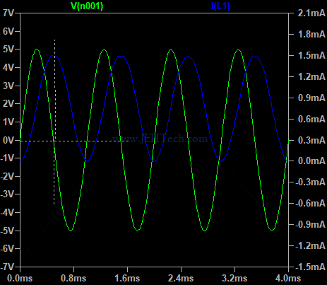
For inductors think ELI - Voltage leads current, or put another way current lags voltage:
Inductors In Series
Inductors In Parallel
Inductors & Capacitors Together
See #55: Back to Basics: Tutorial on LC Resonant Circuits. Really good video!
Current And Voltage Lead And Lag
Helpful: "ELI the ICE man":
Inducance, EMF (V) leads current (I). Or current (I) lays EMF (V).
Capacitance, current (I) leads EMF (V).
Series Resonance
At resonance a series circuit looks like a short circuit.
Resonance occurs when the inductive reactance equals the capacitive reactance:
Parallel Resonance
At resonance a parallel circuit looks like an open circuit.
Reistance, Reactance and Impedance
Refs:
- What's the difference between resistance, reactance, and impedance? -- Danielle Collins. .
- Induction and Inductance -- Iowa State Univeristy.
- Circuits and Phase -- Iowa State Univeristy.
Reactance
Reactance: Property of opposing current change and is therefore specific to AC power and depends on rate of change, i.e., frequency, of current. Creates 90 degree phase shift between voltage and current. This is unlike resistance that constantly opposes current flow, regardless of change - i.e., is not frequency dependent.
Two types:
-
Inductive reactance:
So the reactance, or opposition to change in current, increases with signal frequency and/or inductance-value for an inductor.
See also Inductive Reactance Tutorial.
-
Capacitative reactance:
So the reactance, or opposition to change in current, decreases with signal frequency and/or capacitance-value for a capacitor.
Impedance
Impedance is resistance plus reactance (both inductive and capacitative). It is the total opposition that a circuit presents to
althernating current. It is an imaginary number, where real part is resistance and imaginary part is reactance:
Total impedance is a vector sum because reactance is 90 degrees out of phase with resitance. This vector addition is required.
Diodes
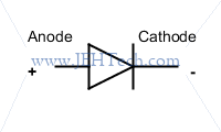
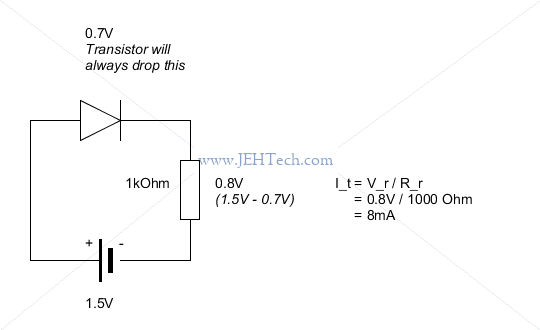
Diodes let current flow in one direction, but not the other, and always drop the same voltage across them no matter the src voltage.
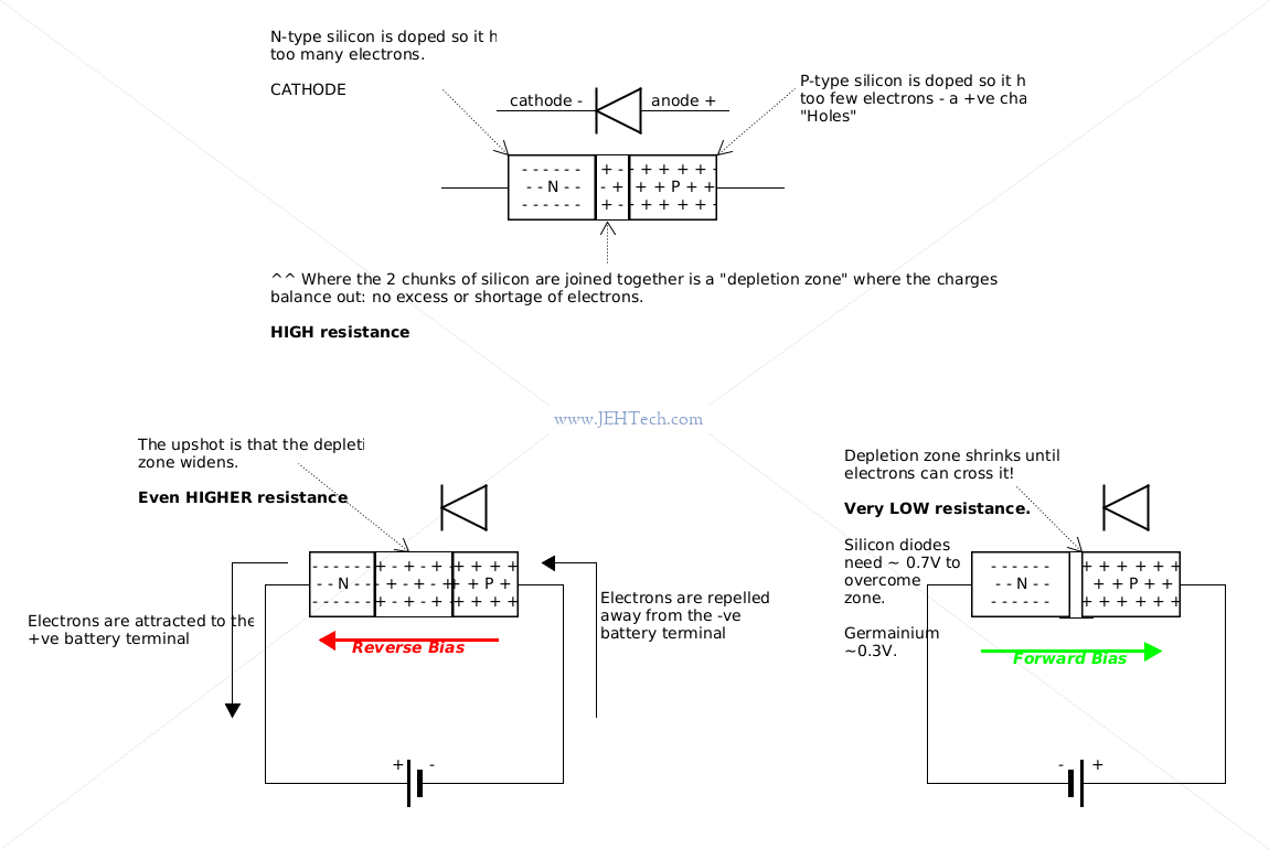
Diodes drop the same voltage across them no matter the voltage source rating. So, for example, silicon diode needs about 0.7V to fwd bias, but won't let the voltage drop across it exceed this. So if you don't protect it with a resistor it will allow too much current to flow and potentially overheat!
Forward and Reverse Voltages - Some Terminology
The forward voltage is the voltage drop across the diode if the voltage at the anode is more positive than the voltage at the cathode (if you connect + to the anode). [I.e., voltage drop when forward biased.] You will be using this value to calculate the power dissipation of the diode and the voltage after the diode. The reverse voltage is the voltage drop across the diode if the voltage at the cathode is more positive than the voltage at the anode (if you connect + to the cathode). [I.e., voltage drop when reverse biased.] This is usually much higher than the forward voltage. As with forward voltage, a current will flow if the connected voltage exceeds this value. This is called a "breakdown". Common diodes are usually destroyed but with Z and Zener diodes this effect is used deliberately.
Light Emitting Diode (LED)
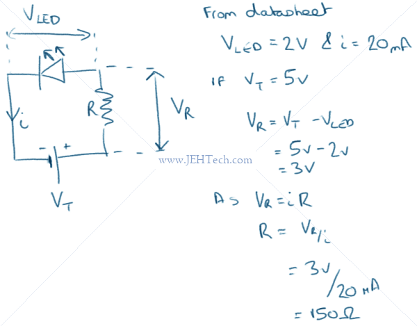
Lets look at a standard red LED datasheet:
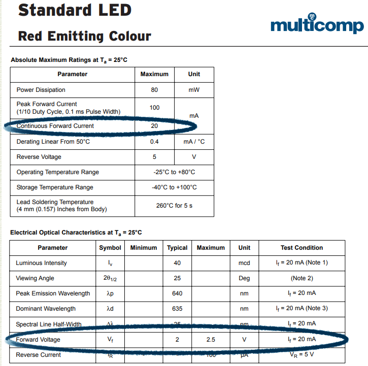
The data sheet shows that we should be putting about 20mA through the LED, with about 2V across it.
That data sheet also shows us that if we reverse bias the LED and put more than 100 micro-amps through it it will break down.
Let's try figuring out some values for a really simple circuit:
Zener Diode
The circuit symbol is:
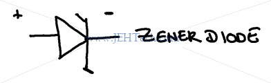
Designed to work in reverse bias in order to maintain a certain voltage. Unlike a normal diode, which
will not conduct when reverse biased, the Zener diode does, at a very specific breakdown voltage
called the Zener voltage,
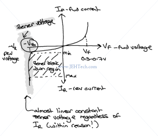
Zener diodes must always be used with a resistor in seriers to limit the current.
A common use is as a voltage regulator:
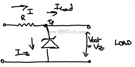
As the load increases (i.e., the load resistance increases), more of
To do this, the zener must sink more current because
That that when used this way, if the input voltage is lower than
Be careful with Zener power rating. You must pick a Zener diode to match the voltage/current it is coping with!
When forward biased the Zener just works like a normal diode, but is not really used like this.
For super gorey details on Zeners and TVS devices see TVS/Zener Theory and Design Considerations Handbook.
Schottky Diode
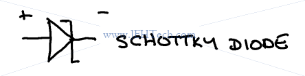
Much lower "on" voltage required so dissipates less power but has higher leakage current if reverse biased.
References
- Diodes and Diode Circuits.
- Accounting for LED resistance, StackExchange.
Bipolar Junction Transistors (BJT)
BJT transitors typically come in a TO-92 package, where "TO" stands for "Transitor Outline". The are many TO package types available.
NPN Transistor in Common Emitter Configuration
NPN transistors consist of two N-type (negatively doped - excess electroncs) silicon "chunks" sandwiching a P-type (positively doped - exess holes or lacking electrons) as shown below. They are current controlled.
And now some help from my good friends ChatGPT:
By forward biasing the emitter to base junction with even a small current, the transistor's resistance between the emitter and collector quickly decreses, allowing a relatively large current to flow from the emitter to collector. I.e., base current controls current at emitter and collector.
A BJT works by controlling how many charge carriers move through the base region. The base current injects these carriers. More carriers means more collector-to-emitter current can flow. That's why Ic follows Ib.
When you put current into the base, you inject charge carriers (electrons or holes depending on NPN/PNP). These carriers spread into a thin region inside the transistor. That region is like a "valve body". The collector-emitter current is basically how many of those carriers are available for the collector to "pull" across.
- The base current fills the base region with carriers.
- The collector voltage pulls those carriers across the junction.
- The more carriers you’ve injected, the more current the collector can draw.
- When the collector tries to draw more current than the injected carriers allow, the transistor limits the current.
Note that the base current does not supply all the carriers that flow as collector current. It only seeds the region with enough carriers so the collector-emitter path can pull in many more from the emitter. In other words, most of the carriers that make up the collector current actually come from the emitter, not the base. The base current just makes the junction "open enough so the emitter can supply a much larger flow.
Understand that
Where Is is the leakage current, which is extremely small (nanoamps or less). Vt is the thermal voltage.
Basically, the voltage controls the current in an exponential way with Is scaling the current through the diode and Vt setting the rate of rise.
In practice, don't use the diode equation just that you need:
- about 0.6 to 0.7 V for a silicon transistor when it's on
- maybe 0.75 to 0.85 V if the current is high
- maybe 0.5 to 0.55 V if the current is tiny
--- End ChatGPT content.
The circuit in its most basic form looks like:
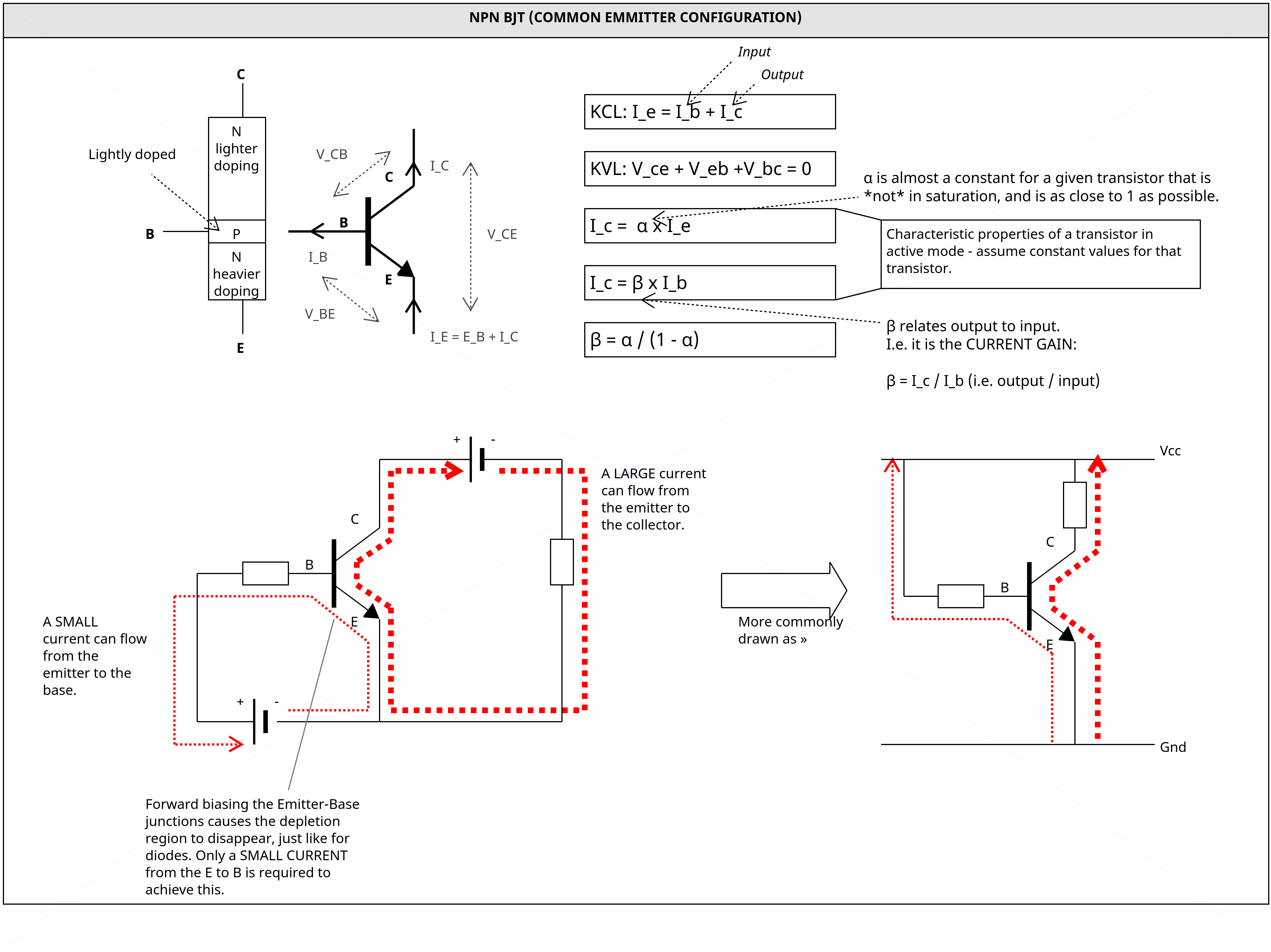
- The base is responsible for initiating transistor action. When a voltage is applied at the base, it gets biased and draws small current which is then used to control large current at the collector and emitter side.
- The base action is considered as an ON-OFF valve which generates current when a proper bias voltage is applied at this terminal.
- The small change at the voltage applied at the base terminal shows a large impact at the output terminals. Actually, base acts as an input and collector acts as an output in NPN transistor.
- In case of silicon transistor emitter-base junction draws voltage around 0.7V when there is no voltage at the base terminal, in order to initiate the electron action and put the transistor in running condition, the base voltage must be greater than 0.7 voltage in case of silicon transistor and 0.3 in case of germanium transistor.
I like this explanation by "Papabravo" on All About Circuits (emphasis mine):
Like a conventional diode the Base-Emitter junction becomes saturated when the voltage difference between the base and the emitter is greater than about 0.7V. It is very difficult to further increase the voltage across the junction because the current increases exponentially for small increases in Vbe. That's the how. The why is related to the behavior of a p-n junction according to the diode equation. If you try to force more than Vbe(sat) across the junction then the device will conduct enough current to destroy itself. That is the principal reason for the base resistor in switching circuits: to limit the base current.
The Art Of Electronics has this to say about
An important warning: the current gain β is not a "good" transistor parameter; for instance, its value can vary from 50 to 250 for different specimens of a given transistor type. It also depends on the collector current, collector-toemitter voltage, and temperature. A circuit that depends on a particular value for beta is a bad circuit.
Thus the emitter voltage is effectively fixed by the base voltage as
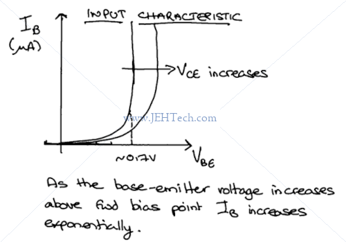
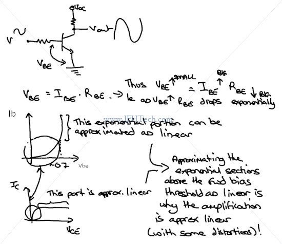
The input characteristics:
The output characteristics:
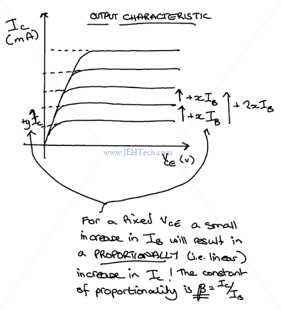
This idealised transistor has horizontal linear regions, which are an approximation of a real
transistor (see below). In the linear region, the transitor is acting like a constant current source
controlled by the base current
The above is for an idealised transistor. Below is a scrape of the semtech 2N2222 datasheet, which shows what it is like for a real transistor:
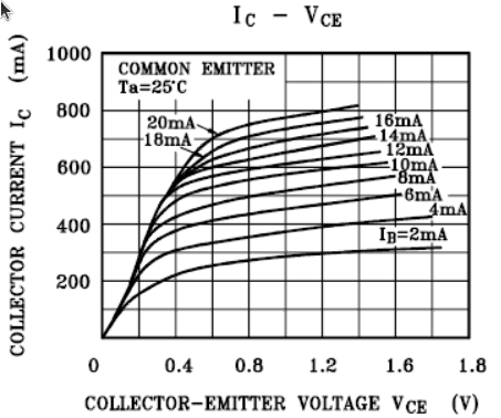
One can see that the amplification isn't linear across the entire range of IB currents. Eye-balling the graph, it looks most linear between 10mA and 16mA...
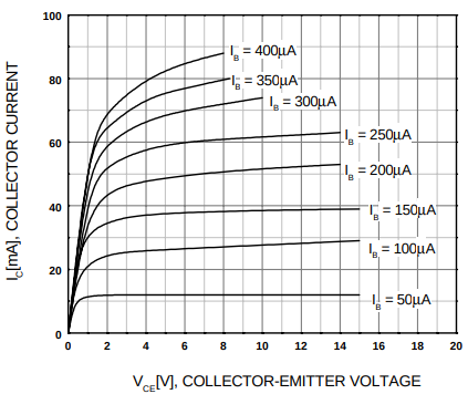
As another example here is the same curve for the BC54x transitor family:
One might wonder, if the input characteristic shows an expenential increase in
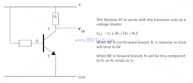
Looking at output is terms of a voltage divider:
The above configuration is called the common emitter configuration and is probably the most widely used [Ref].
The configuration in which the emitter is connected between the collector and base is known as a common emitter configuration. The input circuit is connected between emitter and base, and the output circuit is taken from the collector and emitter. Thus, the emitter is common to both the input and the output circuit, and hence the name is the common emitter configuration.
NPN transistors can typically handle up to about 0.8 A. They will also have a maximum power rating - the average small transistor can only handle about 250mW of heat dissipation. Thus, they are low current devices. For large currents MOSFETs are used (later section).
Saturation region is where the maximum collector current flows and the transistor is basically a closed switch from collector to emitter. The collector-emitter voltage (VCE) is relatively low, and the collector current (IC) becomes nearly constant regardless of further increases in base current (IB). Saturation is often desired in switching applications to ensure the transistor is operating in its fully conducting state.
Active mode / region is where there is an almost linear relationship between the terminal currents at the base, collector and emitter. The transistor has some resistance, that is determined by the emitter/base current.
Cut-off region is where the transistor acts like an open switch.
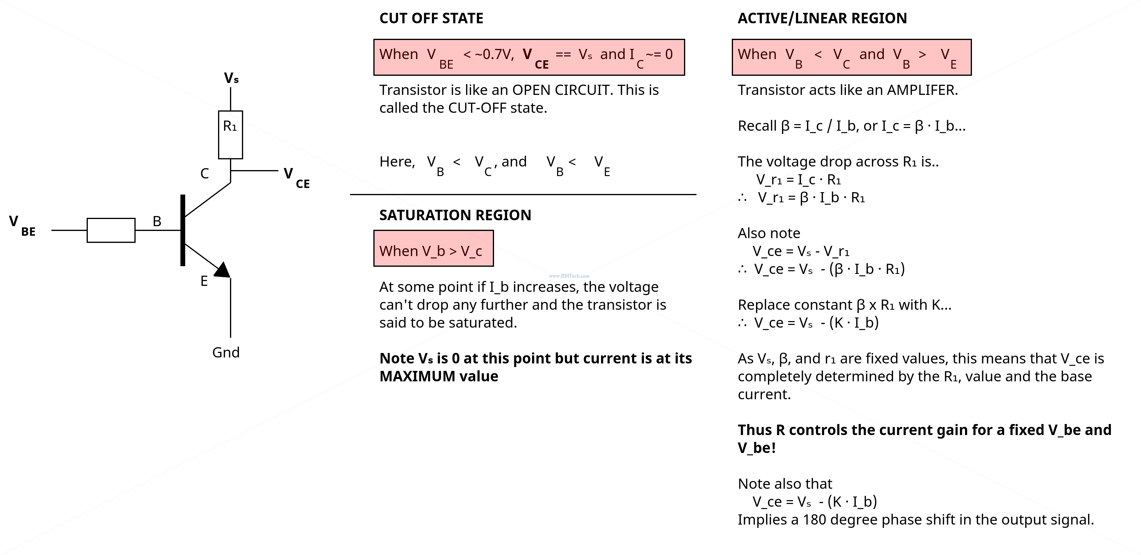
The Khan Achademy has a really really good explanation of saturation, and the following scribble is just a rip of that example:
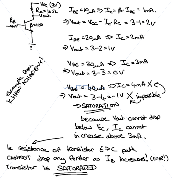
A common NPN transistor is the 2N2222. Looking at the data sheet [Ref] we can find the following properties:
| Parameter | Max |
| Collector-base voltage VCBO | 60 V |
| Collector-emitter voltage VCEO | 30 V |
| Emitter-base voltage VEBO | 5 V |
| Peak collector current | 800 mA |
| Peak base current | 200mA |
| Total power disipation | 500 mW |
We can see that this device can handle a maximum of 0.8A though its emitter-collector and only 0.2A at the base. It is however, able to tolerate relatively high voltages, just not high currents, which as we said above, you'd need MOSFETs, or even relays for.
Other useful numbers from the datasheet include:
| Parameter | Max |
| VCEsat Voltage from collector-emitter when saturated (i.e fully on) | 400mV |
| VBEsat Voltage from base-emitter when saturated (i.e fully on) | 1.3V |
|
HFE DC current gain @ IC = 0.1 mA; VCE = 10 V @ IC = 1 mA; VCE = 10 V @ IC = 10 mA; VCE = 10 V @ IC = 150 mA; VCE = 1 V @ IC = 150 mA; VCE = 10 V |
35 50 75 50 100-300 |
Current Amplification Factor:
The current gain from Collector (C) to Emitter (E): i.e., the ratio of change in collector current to
the change in emitter current when emitter voltage is kept constant:
Ah, it seems
Ratio of output and input current in CE config:
The two are related as follows:
And,
Some examples, taken verbatim, from electronics-tutorials.ws on the NPN Transitor will help understand why these are useful.
A bipolar NPN transistor has a DC current gain,
Calculating Resistor Values
Example 1
All based on an answer from StackOverflow [Ref].
![]()
Example 2
In the following example a transistor is being used to drive a load rated at 6V, 500mW.
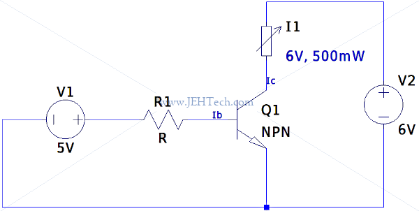
If the load should dissipate 500mW at 6V, this means that the current through it, and
thus the collector current,
Because the base must be 0.7V above the emitter (standard for a transistor but look at the datasheet),
we know the resistor must frop 4.3V. Thus we can calculate the resistance:
Common Emitter Amplifer
The common emitter amplifier provides voltage gain and moderate current gain [Ref]. It inverts the signal at the input, i.e., it has 180 degree phase change from input to output.
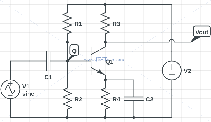
In the above, C1, known as an AC coupling capacitor, removes any DC component from the input signal, so that the voltage divider at Q can set a DC offset to the signal. This is so that the transistor can be biased to the Q-point, which is a point in the middle of its linear region.
C2, known as an AC coupling capacitor, removes the DC component on the output.
C1 and C2 must be configured to provide negligable reactance (AC resistance) at the frequencies of operation.
C3 is a bypass capacitor that helps enable greater levels of AC gain to be achieved because R4 reduces the current gain.
R4 is rather special. This SO post explains it:
If you didn't have an emitter resistor ... then you'll find that temperature effects will be surprisingly high and the desired 6 volts at the collector may drift with temperature a few volts this way and that way.
This is why the originally referenced article describes R4 as providing ... a measure of DC feedback to ensure that the DC conditions within the circuit are maintained ...
Characteristics:
- Voltage gain == Medium
- Current gain == Medium
- Power gain == High
- Input / output phase relationship == 180 degrees
- Input resistance == Medium
- Output resistance == Medium
References
- Electricity & Electronics - Robotics, Learn By Building, Ian Juby on Udemy.
- NPN Characteristic Curves.
- Introduction To The NPN Transistor, TheEngineeringProjects.com.
- Transistor Configurations: Circuit Configurations, Electronics-Notes.com.
- NPN Transistor 2N2222 DataSheet.
- Calculating resistor value for transistor, StackExchange.
- Common Emitter Connection (or CE Configuration), Ciruit Globe.
- Active, staturation, and cuttof state of NPN transistor, Khan Achademy
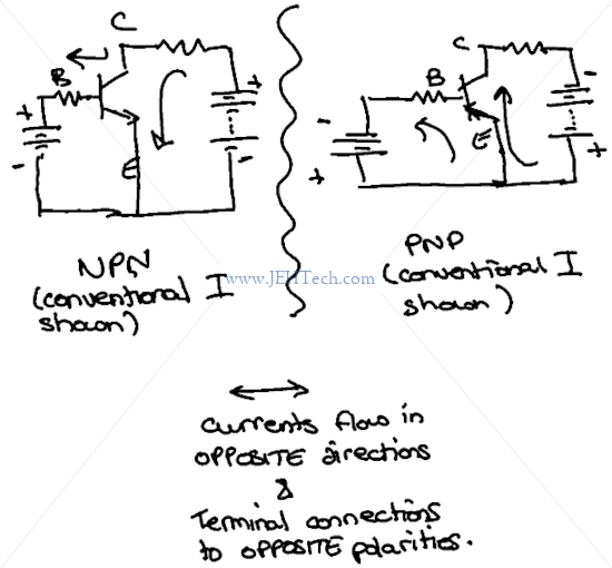
PNP Transistor
Some Examples Bringing Together What We've Seen So Far...
![]()
To turn on the PNP transistor, unlike the NPN, where real, i.e not conventional, current flows from the emitter to the base, with the PNP the real current must flow from the base to the emitter.
Metal Oxide Semiconductor Field Effect Transistor (MOSFET)
N-channel mosfets are also referred to as "nMOS" and P-channel mosefets as "pMOS".
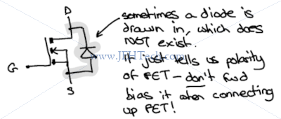
Sometimes you may see a little diode connecting the source to the drain. The diode isn't really there, it is just indicating the polarity of the FET, the idea being you do not connect it so that the imaginary diode is forward biased!
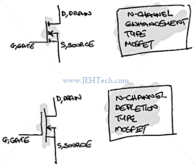
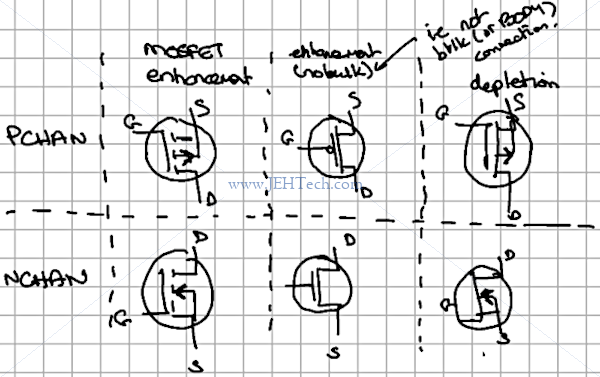
MOSFETs come in the following types:
- N-channel, enhancement mode.
- N-channel, depletion mode.
- P-channel, enhancement mode.
- P-channel, depletion mode.
"Enhancement;" means that a voltage needs to be applied to the gate to "turn it on", whereas "Depletion;" means that a voltage needs to be applied to the gate to "turn it off". N and P type defer to the dopings of the source/drain and body.
The enhancement mode MOSFET symbols use dotted lines to indicate that the channel is "broken" before gate voltage is applied.
- If it is an N-type enhancement mode MOSFET then gate voltage is required to turn it on.
- If it is a P-type enhancement mode MOSFET then gate voltage is required to turn it off.
Depletion mode MOSFET symbols use solid lines to indicate that the channel exists before a voltage is applied to the gate. They are rare in use apparently? For example, LT-spice has no built in deletion mode MOSFET models.
A summary of the various symbols:
An N-type enhacement mode FET's construction is represented in the diagram below:
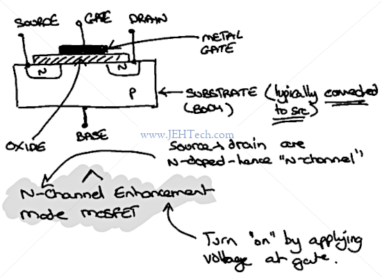
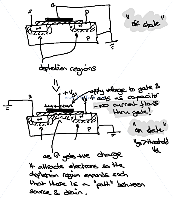
When a voltage is applied to the gate it acts as a capacitor: no current flows through the gate.
But, the accumulation of positive charge at the gate attracks negative charges causes a channel or
"wedge" to be "opened" between the source and drain through which current can flow.
The current flow starts when the gate voltage exceeds the threshold voltage, ie when
.
[Ref].
The input/output characteristics are very similar to the BJTs discussed in the previous section:
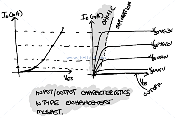
The FET has three modes of operation and annoyingly the terminilogy does not match that used for the BJTs so it can be a little confusing:
- Saturation: In this mode the FET acts as an amplifier. Note this is not the same meaning as saturation in a BJT!!!
- Ohmic: The FET acts like a (voltage controlled) resistor.
- Cut-off: The FET acts like an open circuit.
In an N-channel MOSFET, used in the normal way (low-side switch), conventional current goes from drain to source.
For a P-channel MOSFET the normal current direction is the opposite. Conventional current flows from source to drain in a P-channel device.
The simples model of a FET is:
MOSFETs require pull up/pull down resistors because the gate acts as a capacitor, and when the MOSFET is turned off, the current needs somewhere to dissipate, otherwise the gate would just float!
Enhancement mode, N-type needs a pull down:
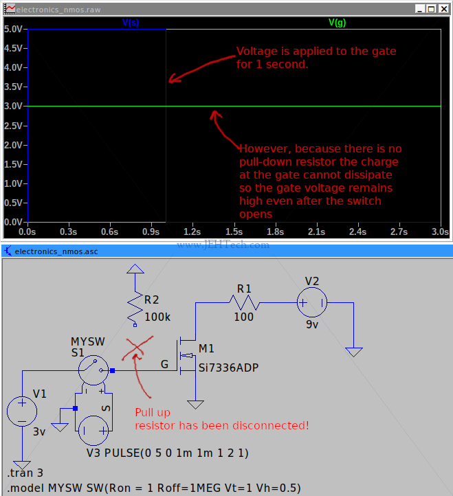
Generated from electronics_nmos.asc
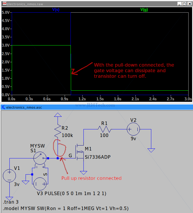
Generated from electronics_nmos.asc
P types will need a pull up resistor, not showing an example here.
Sometimes a current limiting resistor for the gate is required. Because the gate acts as a
a capacitor the current at time
If whatever is driving the gate can supply currents large enough to damage the FET then a gate resistor should be used. it should be positioned to the "right" of the pull up/down resistor so that no voltage divider is created and the gate still receives (most of) the full voltage.
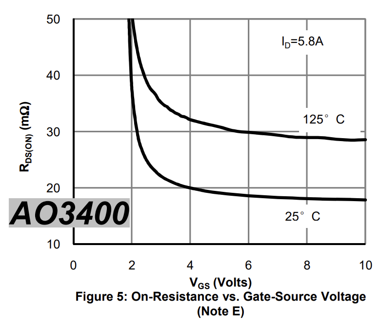
When driving MOSFETs as an on/off switch take note of the VGS and the RDS(on):
NMOS and PMOS Pairs In Logic Gates
I stubled across the following whilst reading up on logic gates using MOSFETS:
A further distinction between NFETs and PFETs is that NFETs are good at discharging capacitive
loads to Gnd but not too good at charging capacitive loads to Vdd, whereas PFETs are good at
charging capacitive loads to Vdd but not too good at discharging capacitive loads to Gnd.
[REF].
Put another way, an NMOS gives a strong 0 but a weak 1 and a PMOS gives a strong 1 but a week 0.
Interesting! Thats why there are often complementary P and N types in logic gates that are implemented using MOSFETs. But why are NFETs good at discarghing capacitive loads and PFETs good at charging them? The answer is here.
MOSFET Drivers
A MOSFET driver IC (like the ICL7667 you mentioned) translates TTL or CMOS logical signals to a higher voltage and higher current, with the goal of rapidly and completely switching the gate of a MOSFET.
An output pin of a microcontroller is usually adequate to drive a small-signal logic level MOSFET, like a 2N7000. However, three issues occur when driving larger MOSFETs:
- Higher gate capacitance - Digital signals are meant to drive small loads (on the order of 10–100 pF). This is much less than the gate capacitance of many MOSFETs, which can be in the thousands of pF.
- Higher gate voltage - A 3.3 V or 5 V signal is often not enough. Usually 8–12 V is required to fully turn on the MOSFET.
- A switching MOSFET can cause a back-current from the gate back to the driving cicruit. MOSFET drivers are designed to handle this back current. (Ref: [Laszlo Balogh Design And Application Guide For High Speed MOSFET Gate Drive Circuits](https://kidbots.com/WEBADD/HYDROGEN_FUEL/slup169.pdf).)
Finally, many MOSFET drivers are designed explicitly for the purpose of controlling a motor with an H-bridge.
Buffers
Why buffers? To isolate one part of a circuit from another. For example, if the output of part A of the circuit is high impedance and is input to part B, which is low impedance then there will be a loss of voltage signal. [Ref] Overcome this with a buffer, which will have a low impedance output.
Inverting Buffer
What suprised me about the inverting buffer, as an electronics newbie trying to teach himself, was that when the input is high, the base current flows from the base to the collector, rather than the emitter because the BC junction becomes forward biased.
MOSFETs vs BJTs
| Characteristic | BJT | MOSFET |
| Type of input signal needed to operate | Current. Whatever provides the input signal must be able to deliver enough current. |
Voltage. The voltage neededd to turn on a MOSFET is about 2V, so the input signal needs to be able to provide a voltage greater than this. No current is drawn by the MOSFET - it is said to have a high input impedance. |
| Peculiarities | None. | Static sensitive and can behave irratically if the gate is left floating. |
| Efficiency | High. The BJT does not waste a lot of power (i.e. get hot). |
Lower. Although rarely a problem, the MOSFET can waste power if it gets hot. |
555 Timer
Introduction
The 555 timer can generate single pulses (monostable) or a train of pulses (astable), acting as an oscillator.
The TI LM555 datasheet gives a a good summary of the internals:
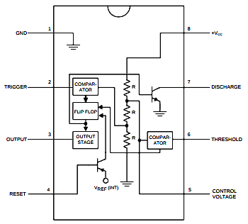
With the following pin descriptions.
| Pin No | Pin Desc | I/O | Description |
| 5 | Ctrl Voltage | I | Controls the threshold and trigger levels. It determines the pulse width of the output waveform. An external voltage applied to this pin can also be used to modulate the output waveform |
| 7 | Discharge | I | Open collector output which discharges a capacitor between intervals (in phase with output). It toggles the output from high to low when voltage reaches 2/3 of the supply voltage. |
| 1 | GND | O | |
| 3 | Output | O | |
| 4 | Reset | I | Negative pulse applied to this pin to disable or reset the timer. When not used for reset purposes, it should be connected to VCC to avoid false triggering. |
| 6 | Threshold | I | Compares the voltage applied to the terminal with a reference voltage of 2/3 Vcc. The amplitude of voltage applied to this terminal is responsible for the set state of the flip-flop. |
| 2 | Trigger | I | Responsible for transition of the flip-flop from set to reset. The output of the timer depends on the amplitude of the external trigger pulse applied to this pin. |
| 8 | Vcc | I |
Monostable
In the monostable mode, the 444 operates as a "one shot" pulse generator...
God bless LT-Spice... below is a sumulation of a 555 in monostable mode. Note, I could have gotten rid of S1 and just used a pluse from V2... I was copying an example with a manual switch and needlessly tried to keep a physical switch in there.
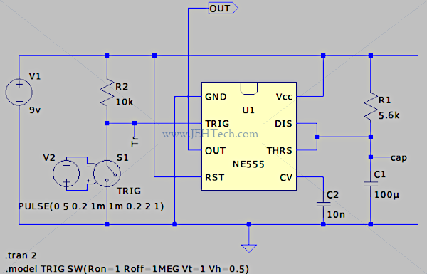
Generated from electronics_555_monostable_1.asc
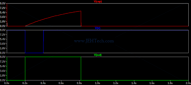
Generated from electronics_555_monostable_1.plt
- The trigger starts the process: it is pulsed low (falling edge triggered) for a short amount of time to kick things off and turn the output on.
- Capactitor C1 begins to charge.
- The threshold pin compares the voltage applied to the terminal with a reference voltage of 2/3 Vcc.
- When the voltage across C1, i.e., the voltage at the threshold pin, is 2/3 Vcc the output is turned off and the capacitor discharges through the discharge pin.
Going into slightly more detail, looking at the LM555 excerpt above, the trigger resets the flipflop, which turns on the output stage.
At this point the discharge transistor will be an open circuit, so the capacitor connected between ground and the joined threshold and discharge pins can charge through the resistor.
As the capacitor charges to above 2/3 Vcc, the comparitor on the threshold pin signals the flipflop, which turns the output off and turns the transitor at the discharge pin on. Pin 7 goes from high impedance to an open circuit so the capacitor is now connected to ground and discarges immediately.
By the way, the only reason the pulse from the 555 is delayed is because the switch closing, i,e the trigger, is delayed by 0.2ms.
Capactitor C2 is used to suppress noise on the control voltage pin. Resistor R2 is a pullup resistor so that the trigger does not float.
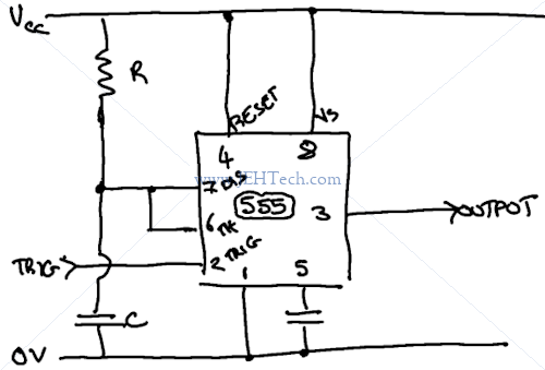
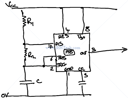
The LTSpice 555 symbol makes for a slightly cumbersome circuit diagram. It is more commonly, and more cleanly, layed out like this:
Calculate Output Period
Recall from the capacitance section that
When a capacitor, with a capacitance
The 555 waits for the capacitor to charge to two thirds, or 66% of the supply voltage. So
Astable
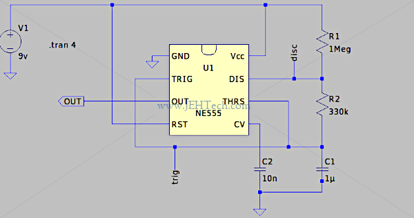
Generated from electronics_555_astable_circuit.asc
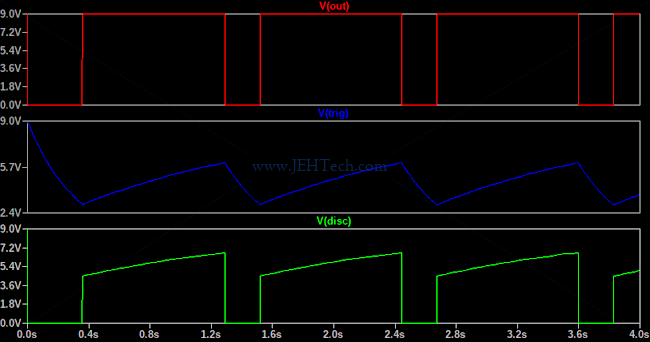
Generated from electronics_555_astable_graph.plt
Above one can see that the system oscillates "by itself". The trigger is "automatic".
- The output stage is initially off because the trigger is high. The discharge transitor on the discharge pin is a closed circuit.
- This means that capacitor C1 can discharge through the resistors R2 into the discharge pin, which is providing a path to ground.
- The trigger and threshold pins "sees" the voltage across C1 and as it falls as the capacitor is discharged. The threshold pin, at this point, won't do anything because it only sets the flipflop, which it already is. It is the trigger pin that, upon hitting 1/3 Vcc, will reset the flipflop. At this point the output does high and the discharge pin becomes high impedance, like an open circuit.
- The capacitor C1 now begins to charge through resistors R1 and R2.
- As the capacitor charges, when it reaches 2/3 Vcc, the threshold pin will set the flipflop, which will turn the output off and open the discharge pin again.
- The process repeats ad infinitum...
The LTSpice 555 symbol makes for a slightly cumbersome circuit diagram. It is more commonly, and more cleanly, layed out like this:
The total resistance R1 + R2 will determine the time it takes for the capacitor to charge. However, when the capacitor discharges, it only discharges through R2.
Recall charge time for a cap to charge to 63% of the voltage across is is
The following is a silly little animation of the capacitor discharging through R2. Imagine that the 3 red dots represent the flow of electrons from the negatively charged plate to the positive plate of the capacitor as it discharges. I think normally it would be shown using conventional current flow, but this animation uses actual electron flow. meh.
Wikipedia has a really nice illustration of the components in the 555, which I've copied below and inserted the components outside the chip that we used above to create an astable vibrator. Here, we can see that the switch shown above is really an RS flip flop combined with a transitor.
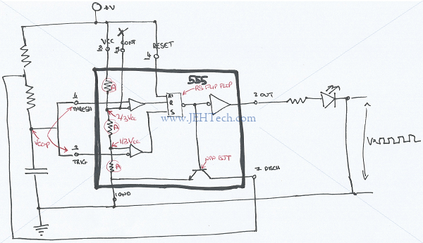
Each of the components, like the RS flip flop, comparitors and other gates can be further broken down into their transitor/resitor combinations, so the above is just another, slightly more detailed abstraction. The real circuit is far, far more complex when broken down into its "atomic" building blocks!
555 References
- 555 Timer IC - Working Principle, Block Diagram, Circuit Schematics, Dejan, Mechatronics How To.
- NE555 Block Diagram, BlanchardJ / Public domain.
- Sequential Logic Circuits, Electronic Tutorials, SR Flip Flop.
- NAND gate, WikiPedia.
Logic Gates
NAND
Using BJTs
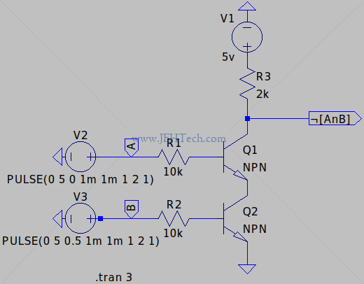
Generated from electronics_bjt_nand_gate.asc
Generated from electronics_bjt_nand_gate.plt
For the voltage at the output to be low there must be a path to ground such that all the voltage gets dropped across R3. This can only happen when both transistors are on, which occurs when both bases, inputs A and B, are high. Hence the NAND gate...
Using MOSFETs
A little more complicated in the MOSFET world!
Set-Reset (SR) Latch
The Set-Reset (SR) latch has the following symbol:
It has the following states:
Decibels
- Are a consistent way to compare signal strengths.
- Are a ratio of two power values.
- Uses logarithmic values so large and small ratios alike can be worked with.
- 1 Bel == x10 power gain or loss. Too big for most measurements, hence the decibel (dB) which is x0.1 power gain or loss.
If the reference power is 1, then,
| Measured power | Gain in dB |
| ... | ... |
| 0.001 | -30 |
| 0.01 | -20 |
| 0.1 | -10 |
| 1 | 0 |
| 10 | 10 |
| 100 | 20 |
| 1000 | 30 |
| ... | ... |
If the measured signal is 10 time stronger than the reference then the gain is 10 dB. If the measured signal is 100 times stronger than the reference then the gain is 20 dB and so on... I.e., +10dB means x10 power gain.
+10dB means x10 power gain.
Note that the decibels difference between two voltage or currents is:
Specific Reference Values
EMI
See Common Mode Chokes Basics and Applications, by Ahmed Alamin, Associate Product Engineer, Abracon, LLC.
Electromagnetic interference (EMI) corresponds to the unwanted electromagnetic
disturbance or noise signal that is introduced in electronic systems by external
or internal sources. These sources can be other systems in the vicinity, such as
radio transmitters, power grid systems, cell phones, switching power supplies,
electrical motors, or even natural sources such as lighting and solar flares
-- [Ref].
Common Mode Chokes
A common mode choke is a passive electromagnetic device that permits the passage
of the desired electrical signals through data or power lines while filtering out
the unwanted high-frequency noise signal from external sources or other circuits of the system.
-- [Ref].