ST Nucleo Notes
Page Contents
Intro
- ST Nucleo F401RE
- Uses the STM32F401RET6 32-bit ARM Cortex M4 CPU:
- 512kB Flash.
- 96 kB RAM.
- See the STM32401xE datasheet.
- See the RM0368 Reference manual for STM32F401xB/C and STM32F401xD/E advanced Arm-based 32-bit MCUs.
- Uses the STM32F401RET6 32-bit ARM Cortex M4 CPU:
- ST Nucleo L552ZE
- 32-bit ARM Cortex M33
- Awesome example code by some chap called Matej Blagsic.
Busses
Straight from the manual:
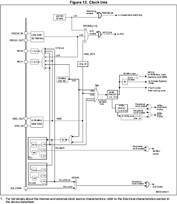
Clock Tree
Straight from the manual:
Debugging
- The STM32Cube IDE uses the STLink GDB server, but I cannot find this as an independent package to install, without installing all of the STM32Cube IDE.
- Note the "ST-link server" and "ST-link DGB server" are not the same thing! [Ref].
-
For non-STM32Cube IDEs most guides suggest using OpenOCD.
The Open On-Chip Debugger (OpenOCD) aims to provide debugging, in-system programming and boundary-scan testing for embedded target devices.
It does so with the assistance of a debug adapter, which is a small hardware module which helps provide the right kind of electrical signaling to the target being debugged.
Install OpenOCD:
apt-get install openocd -
The Nucleo boards have debug adaptor module on-board (ST-LINK/V2-1 debugger): well, really its an STM32F103C8, which is a very small ARM Cortex-M3 MCU that acts as the debug adaptor. The firmware can be upgraded using the app found here.
Setting Up VSCode
- https://marketplace.visualstudio.com/items?itemName=marus25.cortex-debug
- https://marketplace.visualstudio.com/items?itemName=bmd.stm32-for-vscode
- https://medium.com/@erbo-engineering/using-vs-code-for-embedded-stm32-development-14405ed4ac82
- https://bacelarhenrique.me/2020/03/29/complete-guide-to-stm32-arm-development-on-visual-studio-code.html
- https://lonesometraveler.github.io/2020/03/27/debug.html
Little Bare Metal Examples
Turn On The L2 LED
To discover which GPIO pin the LED is connected to, consult the STM32 Nucleo Board User Manual. From the manual one can see that for the NUCLEO-F401RE board, the user LED (L2) is connection to I/O PA5 (pin 21).
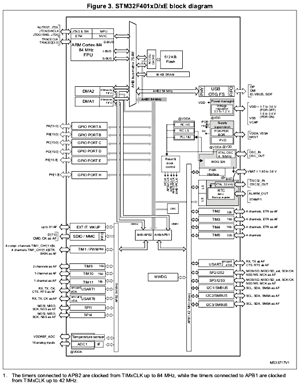
To discover which internal processor bus the GPIO module is attached to consult the STM32401xE datasheet and see Figure 3, the STM32F401xD/xE block diagram. From here one can see that GPIO bank A is connected to the AHB1 bus.
To find out how to enable the GPIO_A bank consult the RM0368 Reference manual, specifically the Reset and clock control (RCC) section for the "RCC AHB1 peripheral clock enable register (RCC_AHB1ENR)" register definition.
The default register value disables all the GPIO modules. It also disables the CRC module and DMA modules.
Thus the GPIO A module must be enabled. Then the LED can be configured:
#include "stm32f401xe.h"

...

/* Enable clock to GPIO_A bank */
RCC->AHB1ENR |= RCC_AHB1ENR_GPIOAEN;

/* Set PA5 to be a general purpose push-pull output type */
/* Make it push pull */
GPIOA->OTYPER &= GPIO_OTYPER_OT5;

/* Make it a general purpose output */
GPIOA->MODER &= ~GPIO_MODER_MODER5;
GPIOA->MODER |= GPIO_MODER_MODER5_0;

/* Now the user LED can be turned */
GPIOA->ODR |= GPIO_ODR_OD5;
Use Serial
To discover which internal processor bus the USART_1 module is attached to consult the STM32401xE datasheet and see Figure 3, the STM32F401xD/xE block diagram. From here one can see that it is connected to the APB2 bus.
To find out how to enable the USART_1 module consult the RM0368 Reference manual, specifically the Reset and clock control (RCC) section for the "RCC APB2 peripheral clock enable register (RCC_APB2ENR)" register definition.